 | –≠–ª–µ–∫—Ç—Ä–æ–Ω–Ω—ã–π –∫–æ–º–ø–æ–Ω–µ–Ω—Ç: THAT4305 | –°–∫–∞—á–∞—Ç—å:  PDF PDF  ZIP ZIP |
THAT Corporation; 45 Sumner Street; Milford, Massachusetts 01757-1656; USA
Tel: +1 508 478 9200; Fax: +1 508 478 0990; Web: www.thatcorp.com
Document 600067 Rev 00
T H A T
C o r p o r a t i o n
Pre-trimmed Analog Engine
Æ
IC
THAT
4305
FEATURES
∑
Pre-trimmed BlackmerTM VCA &
RMS-level detector
∑
Wide supply voltage range:
±4.5V ~±16V
∑
Low supply current:
3.5 mA typ. (±15V)
∑
Wide dynamic range:
117 dB (VCA)
60 dB (RMS-level detector)
APPLICATIONS
∑
Compressors & Limiters
∑
Gates & Expanders
∑
AGCs
∑
Line-operated dynamics processors
∑
De-Essers
∑
Duckers
∑
Mixers
∑
Level indicators
∑
Companding noise reduction systems
Description
The THAT4305 is a single-chip Analog En-
gine optimized for low-cost applications. It incor-
porates a high-performance Blackmer voltage-
controlled amplifier (VCA) and log-responding
RMS-level sensor. The VCA and RMS detector
are pre-trimmed at wafer stage to deliver low dis-
tortion without further adjustment.
Available only in a small (QSOP) surface-
mount package, the 4305 is aimed at line-oper-
ated audio applications such as compressor/lim-
iters, gates, and other dynamic processors. The
part normally operates from a split supply volt-
age up to ±16Vdc, drawing only 3.5mA at ±15V.
This IC also works at supply voltages as low as
±4.5V, making it useful in some battery-operated
products as well.
The 4305 was developed specifically for use
in low-cost dynamics processors, drawing from
THAT's long history and experience with such
designs. Both VCA control ports and the detec-
tor input and output are available for the de-
signer to connect as s/he sees fit. As a result, the
part is extremely flexible and can be configured
for a wide range of applications including single-
and multi-band companders, digital overload
protectors, voltage-controlled faders, level indi-
cators, etc.
What really sets the 4305 apart from other
manufacturers' offerings is the transparent sound
of its Blackmer VCA, coupled with its accurate
true-RMS level detector. This makes the IC useful
in a wide range of analog audio products.
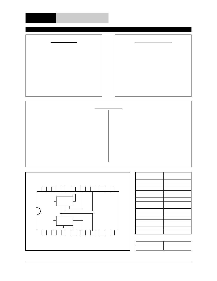
15
2
14
3
13
4
12
5
11
6
10
7
9
8
EC-
EC+
IN
OUT
VCA
IN
CT
OUT
RMS
16
1
VCA
IN
RMS
IN
VCA
OUT
CT
NC
NC
NC
NC
EC-
RMS
OUT
EC+
GND
NC
NC
VCC
VEE
Figure 1. THAT4305 equivalent block diagram
Pin Name
Pin Number
No Connection
1
RMS IN
2
No Connection
3
C
TIME
4
RMS OUT
5
GND
6
NC
7
Vee
8
V
CC
9
No Connection
10
EC+
11
EC-
12
VCA OUT
13
No Connection
14
VCA IN
15
No Connection
16
Table 1. THAT 4305 pin assignments
Package
Order Number
16 pin QSOP
4305Q16-U
Table 2. Ordering Information

THAT Corporation; 45 Sumner Street; Milford, Massachusetts 01757-1656; USA
Tel: +1 508 478 9200; Fax: +1 508 478 0990; Web: www.thatcorp.com
Page 2
THAT4305 Pre-trimmed Analog Engine
Operating Temperature Range (T
OP
)
-40 to +85 ∫C
Junction Temperature (T
J
)
-40 to +125 ∫C
Power Dissipation (P
D
) at T
A
=85 ∫C
400mW
Supply Voltages (V
CC
, V
EE
)
±
18V
VCA Control Voltage
±0.6 V
Storage Temperature Range (T
ST
)
-40 to +125 ∫C
Absolute Maximum Ratings
1
Power Supply
Positive Supply Voltage
V
CC
Referenced to GND
+4.5
-
+16
V
Negative Supply Voltage
V
EE
Referenced to GND
-4.5
-
-16
V
Supply Current
No Signal
I
CC
V
CC
=+15V, V
EE
= -15V
3.5
5
mA
I
EE
V
CC
=+15V, V
EE
= -15V
-3.5
-5
mA
I
CC
V
CC
=+5V, V
EE
= -5V
2
mA
I
EE
V
CC
=+5V, V
EE
= -5V
-2
mA
Voltage Controlled Amplifier (VCA)
Max. I/O Signal Current
i
IN(VCA)
+ i
OUT(VCA)
±1.8
mA
peak
VCA Gain Range
-60
+60
dB
Gain at 0V Control
G
0
E
C+
= E
C-
= 0V
-1.0
0
+1.0
dB
Gain-Control Constant
E
C+
/Gain (dB)
-60 dB < gain < +60 dB
-
6.2
-
mV/dB
Gain-Control Tempco
E
C
/
T
CHIP
Ref T
CHIP
=27∫C
-
+0.33
-
%/∫C
Output Offset Voltage Change
3
V
OFF(OUT)
R
OUT
= 20 k
0 dB gain
-
1
15
mV
+15 dB gain
-
3
30
mV
+30 dB gain
-
10
50
mV
Output Noise
e
N(OUT)
0 dB gain
22Hz~22kHz, R
IN
=R
OUT
=20 k
-
-97.5
-95
dBV
Total Harmonic Distortion
THD
V
IN
= -5dBV, 1kHz, E
C+
= E
C-
= 0V
0.07
0.15
%
RMS level detector
Output Voltage at Reference i
IN
e
O(0)
i
IN
= 7.5
µ
A RMS
-9
0
+9
mV
Output Error at Input Extremes
e
O(RMS)error
i
IN
= 200 nA RMS
±1
±3
dB
i
IN
= 200
µ
A RMS
±1
±3
dB
Scale Factor Match to VCA
-20 dB < VCA gain < +20 dB
1
µ
a< i
IN(RMS)
< 100
µ
A
.95
1
1.05
-
Electrical Characteristics
2
Parameter
Symbol
Conditions
Min
Typ
Max
Units
SPECIFICATIONS
1. If the devices are subjected to stress above the Absolute Maximum Ratings, permanent damage may result. Sustained operation at
or near the Absolute Maximum Ratings conditions is not recommended. In particular, like all semiconductor devices, device reliabil-
ity declines as operating temperature increases.
2. Unless otherwise noted, T
A
=25∫C, V
CC
=+15V, V
EE
= -15V.
3. Reference is to output offset with -60dB VCA gain.
THAT Corporation; 45 Sumner Street; Milford, Massachusetts 01757-1656; USA
Tel: +1 508 478 9200; Fax: +1 508 478 0990; Web: www.thatcorp.com
Document 600067 Rev 00
Page 3
Theory of Operation
The THAT 4305 Dynamics Processor combines
THAT Corporation's proven exponentially controlled
BlackmerTM Voltage-Controlled Amplifier (VCA) and
log-responding RMS-Level Detector building blocks
in a small package optimized for low cost designs.
The part is fabricated using a proprietary, fully com-
plementary, dielectric-isolation process. This pro-
cess produces very high-quality bipolar transistors
(both NPNs and PNPs) with unusually low collector-
substrate capacitances. The 4305 takes advantage of
these devices to deliver wide bandwidth and excel-
lent audio performance while consuming very low
Rectifier Balance
±7.5
µ
A DC
IN
±1
±3
dB
Timing Current
I
T
-
7.5
-
µ
A
Filtering Time Constant
3467 X C
TIME
s
Output Tempco
E
O
/
T
CHIP
Ref T
CHIP
= 27 ∫C
-
+0.33
-
%/∫C
Load Resistance
R
L
-250mV < V
OUTRMS
< +250mV
2
k
Capacitive Load
C
L
150
pf
Electrical Characteristics (con't)
2
Parameter
Symbol
Conditions
Min
Typ
Max
Units
Surface Mount Package
Type
See Fig. 23 for dimensions
16 Pin QSOP
Thermal Resistance
JC
SO package in ambient
105
∫C/W
Thermal Resistance
JA
SO package soldered to board
40
∫C/W
Environmental Regulation Compliance
Complies with RoHS requirements
Soldering Reflow Profile
JEDEC JESD22-A113-D (250 ∫C)
Package Characteristics
Parameter
Symbol
Conditions
Min
Typ
Max
Units
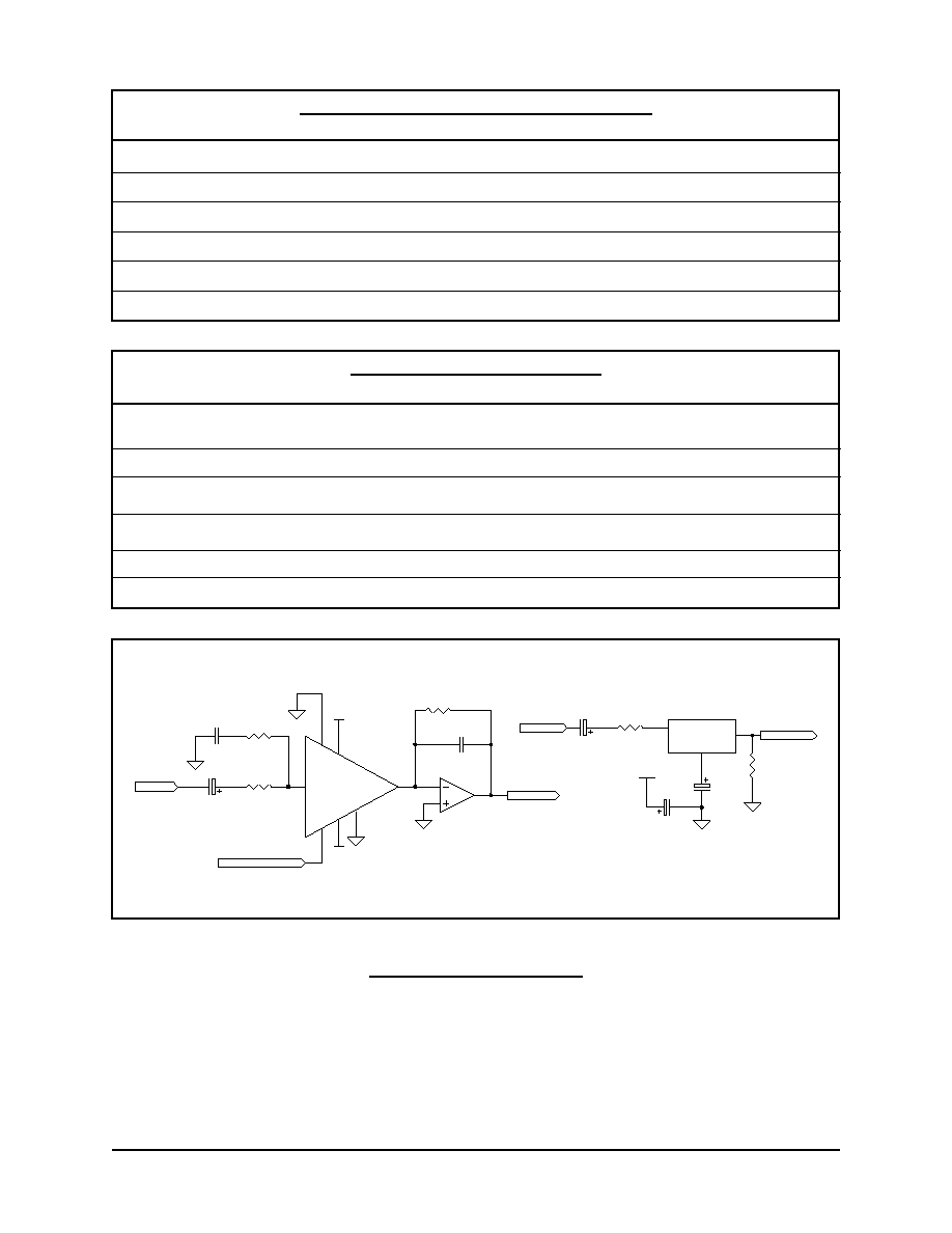
R1
5k1
C1
10u
R2
20k
C3
22p NPO
R3
20k
C2
10u
10u
C5
100p
R4
6k8
VCA Out
13
VCA In
15
U1A
THAT4305
RMS In
2
RMS Out
5
U1B
THAT4305
+15V
-15V
VCA Out
VCA In
RMS In
RMS Out
Control Voltage
U2
R5
2k
Vcc
Gnd
Vee
Ec-
Ec+
9
11
6
8
12
4
CT
C
TIME
C4
10u
+15V
Figure 2. Simplified application circuit

THAT Corporation; 45 Sumner Street; Milford, Massachusetts 01757-1656; USA
Tel: +1 508 478 9200; Fax: +1 508 478 0990; Web: www.thatcorp.com
Page 4
THAT4305 Pre-trimmed Analog Engine
current and operating over a wide range of power
supply voltages.
For details of the theory of operation of the VCA
and RMS Detector, we refer the interested reader to
THAT Corporation's data sheets on the 2180-Series
VCAs and the 2252 RMS Level Detector. Theory of
the interconnection of exponentially controlled VCAs
and log-responding level detectors is covered in
THAT Corporation's application note AN101A, The
Mathematics of Log-Based Dynamic Processors.
The VCA - in Brief
The VCA in the 4305 is based on THAT Corpora-
tion's highly successful complementary log-antilog
gain cell topology (the BlackmerTM VCA) as used in
THAT 2180-Series IC VCAs. VCA symmetry is
trimmed during wafer probe for minimum distor-
tion. No external adjustment is allowed.
Input signals are currents in the VCA's VCA
IN
pin
(pin 15). This pin is a virtual ground with a small dc
offset, so in normal operation an input voltage is
converted to input current via an appropriately sized
resistor (R3 in Figure 2). Because the dc current as-
sociated with dc offsets present at the input pin plus
any dc offset in the preceding stages will be modu-
lated by gain changes (thereby becoming audible as
thumps), the input pin is normally ac-coupled. This
blocks such offset currents and reduces dc offset
variation with gain.
The VCA output signal, VCA
OUT
(pin 13), is also
a current, inverted with respect to the input current.
In normal operation, the output current is converted
to a voltage via an external op-amp, where the cur-
rent-to-voltage conversion ratio is determined by the
feedback resistor connected between the op-amp's
output and its inverting input (R2 in Figure 2). The
resulting signal path through the VCA plus op-amp
is noninverting.
The VCA gain is controlled by the voltage applied
between E
C+
(pin 11) and E
C-
(pin 12). Note that any
unused control port should be connected to ground
(as E
C+
is in Figure 2). The gain (in decibels) is pro-
portional to (E
C+
- E
C-
). The constant of proportion-
ality is 6.2 mV/dB for the voltage at E
C+
(relative to
E
C-
). Note that neither E
C+
or E
C-
should be driven
more than ±0.6 V away from ground.
The VCA's noise performance varies with gain in
a predictable way, but due to the way internal bias
currents vary with gain, noise at the output is not
strictly the product of a static input noise times the
voltage gain commanded. At large attenuation, the
noise floor is usually limited by the input noise of
the output op-amp and its feedback resistor. At 0 dB
gain, the noise floor of ~ -97.5 dBV is the result of
the VCA's output noise current, converted to a volt-
age by the typical 20k I-V converter resistor (R2 in
Figure 2). In the vicinity of 0 dB gain, the noise in-
creases more slowly than the gain: approximately
5 dB noise increase for every 10 dB gain increase.
Finally, as gain approaches 30 dB, output noise be-
gins to increase directly with gain.
While the 4305's VCA circuitry is very similar to
that of the THAT 2180 Series VCAs, there are sev-
eral important differences, as follows.
1. Supply current for the 4305 VCA depends on
the supply voltage. At ±5 V, approximately 800 uA is
available for the sum of input and output signal cur-
rents. This increases to about 1.8 mA at ±15 V.
(Compare this to ~1.8 mA for a 2180 Series VCA
when biased as recommended.)
2. The SYM control port (similar to that on the
2180 VCA) is not brought out to an external pin; it is
driven from an internally trimmed current genera-
tor.
3. The control-voltage constant is approximately
6.2 mV/dB, due primarily to the higher internal op-
erating temperature of the 4305 compared to that of
the 2180 Series.
The RMS Detector - in Brief
The 4305's detector computes RMS level by rec-
tifying input current signals, converting the rectified
current to a logarithmic voltage, and applying that
voltage to a log-domain filter. The output signal is a
dc voltage proportional to the decibel-level of the
RMS value of the input signal current. Some ac com-
ponent (at twice the input frequency plus higher-
order even harmonics) remains superimposed on
the dc output. The ac signal is attenuated by a log
domain filter, which constitutes a single-pole rolloff
with cutoff determined by an external capacitor (C4
in Figure 2).

The rectifier is balanced to within ±3 dB, so a
small amount of fundamental (and higher odd-order
harmonics) ripple can be present at the detector out-
put. By design, this ripple contributes less total rip-
ple than the even-order products that are naturally
and inevitably present at the output of a perfectly
balanced detector.
As in the VCA, input signals are currents to the
RMS
IN
pin (pin 2). This input is a virtual ground, so
a resistor (R1 in Figure 2) is normally used to con-
vert input voltages to the desired current. The level
detector is capable of accurately resolving signals
well below 10 mV (with a 5 k
input resistor). How-
ever, if the detector is to accurately track such
low-level signals, ac coupling (C1 in Figure 2) is re-
quired to prevent dc offsets from causing a dc cur-
rent to flow in the detector's input, which would
obscure low-level ac signal currents.
The log-domain filter cutoff frequency is usually
placed well below the frequency range of interest.
For an audio-band detector, a typical value would be
5 Hz, or a 32 ms time constant (
). The filter's time
constant is determined by an external timing capaci-
tor (C
TIME
) attached to the C
T
pin (pin 4), and an in-
ternal current source (I
T
) connected to C
T
. The
current source is internally fixed at 7.5 µA. The re-
sulting time constant in seconds is approximately
equal to 3467 times the value of the timing capacitor
in Farads. Note that, as a result of the mathematics
of RMS detection, the attack and release time con-
stants are fixed in their relationship to each other.
The RMS detector is capable of driving large
spikes of current into C
TIME
, particularly when the
audio signal input to the RMS detector increases
suddenly. This current is drawn from V
CC
(pin 9),
fed through C
TIME
at pin 4, and returns to the power
supply through the ground end of C
TIME
. If not han-
dled properly through layout and bypassing, these
currents can mix with the audio in the circuit's
ground structure with unpredictable and undesir-
able results. As noted in the Applications section,
local bypassing from the V
CC
pin to the ground end
of C
TIME
is strongly recommended in order to keep
these currents out of the ground structure of the cir-
cuit (see C4 in Figure 2.)
The dc output of the detector is scaled with the
same constant of proportionality as the VCA gain
control: 6.2 mV/dB. The detector's 0 dB reference
(i
in0
, the input current which causes the detector's
output to equal 0V), is trimmed during wafer probe
to equal approximately 7.5 µA. The RMS detector
output stage is capable of sinking or sourcing
125 µA. It is also capable of driving up to 150 pF of
capacitance.
Frequency response of the detector extends
across the audio band for a wide range of input sig-
nal levels. Note, however, that it does fall off at high
frequencies at low signal levels like THAT's other
RMS detectors.
Differences
between
the
4305's
RMS
level
detector circuitry and that of the THAT 2252 RMS
detector include the following.
1. The rectifier in the 4305 RMS Detector is in-
ternally balanced by design, and cannot be balanced
via an external control. The 4305 will typically bal-
ance positive and negative halves of the input signal
within 10 %, but in extreme cases the mismatch may
reach +40 % or -30 % (±3 dB). However, even such
extreme-seeming mismatches will not significantly
increase ripple-induced distortion in dynamics pro-
cessors over that caused by balanced signal ripple
alone.
2. The time constant of the 4305's RMS detector
is determined by the combination of an external ca-
pacitor C
TIME
and an internal current source. The in-
ternal current source is set to about 7.5 µA. A
resistor is not normally connected directly to the C
T
pin on the 4305.
3. The 0 dB reference point, or level match, is
also set to approximately 7.5 µA. However, as in the
2252, the level match will be affected by any addi-
tional currents drawn from the C
T
pin.
Compressor (or Limiter) Configurations
The 4305 provides the two essential building
blocks required for a wide variety of dynamics pro-
cessing applications.
The part may be configured
into practically any type of dynamics processor sys-
tem.
Perhaps the most common application for the
4305 is as a compressor or limiter. These circuits
are intended to reduce gain above some determined
signal level in order to prevent subsequent stages
from being overloaded by too high a signal.
Com-
pressors generally have low to moderate compres-
THAT Corporation; 45 Sumner Street; Milford, Massachusetts 01757-1656; USA
Tel: +1 508 478 9200; Fax: +1 508 478 0990; Web: www.thatcorp.com
Document 600067 Rev 00
Page 5